Double-side
Features manufacture double-side and General tolerances
We classify the circuit difficulty in accordance with the next parameters:
CLASS
Dimensional characteristics of the different elements that form the image of the printed circuit board.
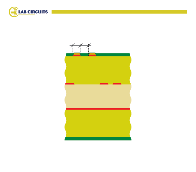
RING CHECK
Copper ring between de hole and the pad. This parameter determinates the alignment difficulty between the hole and the printed circuit board image.
TOLERANCES
Tolerance level of the different proceedings and materials.
The sum of these three items will define the manufacture difficulty and therefore the price of the printed circuit board.

PARAMETERS MANUFACTURE DOUBLE SIDE
| CLASS 3 | CLASS 4 | CLASS 5 | CLASS 6 | CLASS 7 | ||
|---|---|---|---|---|---|---|
| Minimum plated through hole diameter | 
|
0,50 mm | 0,30 mm | 0,30 mm | 0,20 mm | 0,15 mm |
| Minimum non plated through hole diameter | 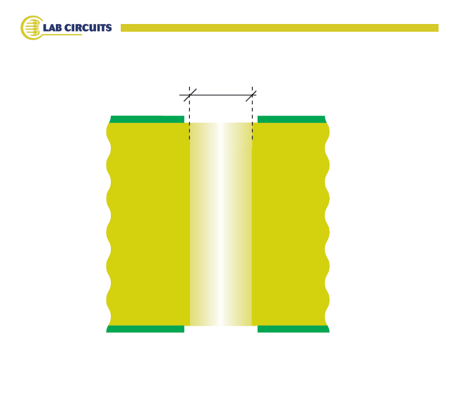
|
0,60 mm | 0,40 mm | 0,40 mm | 0,30 mm | 0,25 mm |
| Aspect / Ratio | 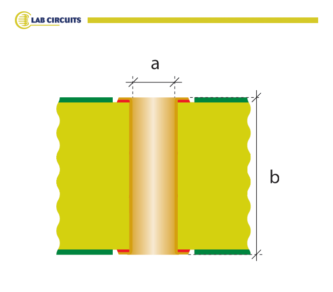
|
5 | 5 | 6 | 8 | 13
(maximum thickness 2 mm) |
| Minimum trace / spacing width (base copper thickness) | 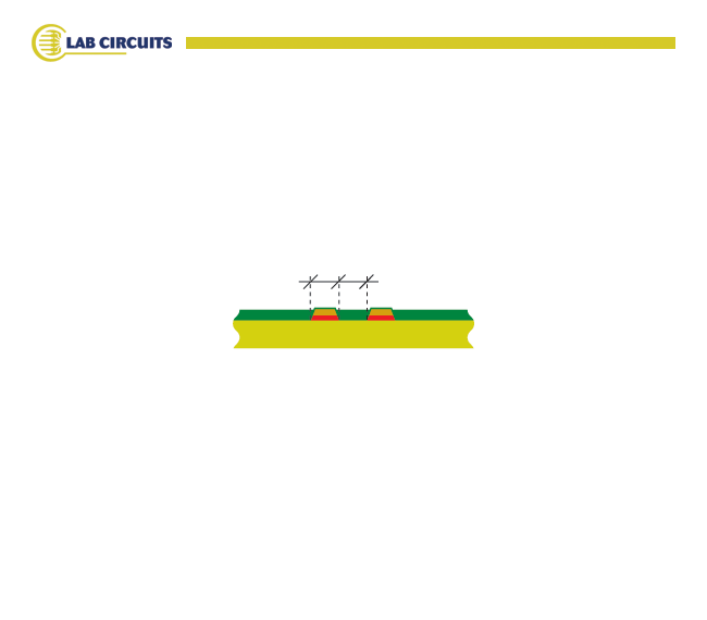
|
0,300 mm (17 µ)
0,300 mm (35 µ) 0,350 mm (70 µ) 0,350mm (105µ) |
0,200 mm (17 µ)
0,200 mm (35 µ) 0,250 mm (70 µ) 0,300mm (105µ) |
0,150 mm (17 µ)
0,150 mm (35 µ) 0,200 mm (70 µ) 0,250 mm (105 µ) |
0,125 mm (17 µ)
0,150 mm (35 µ) 0,175 mm (70 µ) 0,200 mm (105 µ) |
0,100 mm (17 µ)
|
| Minimum annular ring
|
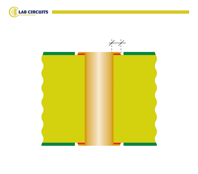
|
0.22 mm | 0.17 mm | 0.13mm | 0.10mm | 0.075 mm |
Last update: 28-04-2023
Units: Milimeters
| CLASS 3 | CLASS 4 | CLASS 5 | CLASS 6 | CLASS 7 | ||
|---|---|---|---|---|---|---|
| Minimum plated through hole diameter |
|
20 mil | 12 mil | 12 mil | 8 mil | 6 mil |
| Minimum non plated through hole diameter |
|
24 mil | 16 mil | 16 mil | 12 mil | 10 mil |
| Aspect / Ratio |
|
5 | 5 | 6 | 8 | 13 (maximum
thickness 2 mm) |
| Minimum trace / spacing width (base copper thickness) |
|
12 mil (½ oz)
12 mil (1 oz ) 14 mil (2 oz ) 14 mil (3 oz ) |
8 mil (½ oz )
8 mil (1 oz ) 10 mil (2 oz ) 12 mil (3 oz ) |
6 mil (½ oz)
6 mil (1 oz ) 8 mil (2 oz ) 10 mil (3 oz ) |
5 mil (½ oz)
6 mil (1 oz ) 7 mil (2 oz ) 8 mil (3 oz ) |
4 mil (½ oz )
|
| Minimum annular ring
|
|
9 mil | 7 mil | 5 mil | 4 mil | 3 mils |
Last update: 28-04-2023
Units: Mils
BILAYER GENERAL TOLERANCES
| STANDARD | SPECIAL | ||
|---|---|---|---|
| Trace / spacing width
(thickness copper foil) |
|
±25% (35-70 µm)
±20% (17 µm ) |
±15% (35-70 µm)
±10% (17 µm) |
| Plated hole diameter | 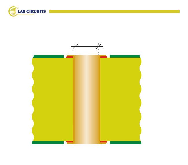
|
+0,10 mm / -0,05 mm
(or equivalent) |
+0,10 mm / -0,0 mm
(or equivalent) |
| Non plated hole diameter | 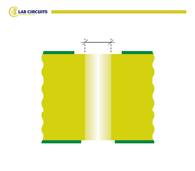
|
+0,10 mm / -0,0 mm
(or equivalent) |
±0,035 mm
(or equivalent) |
| Castellated plated holes | 
|
Total thickness circuit.....................>= 0,5 mm
Cross annular ring.......... detall - A >= 0,5 mm Minimum diameter..........detall - B >= 0,5 mm Longitudinal annular...... detall - C >= 0,15 mm Annular separation.........detall - D >= 0,15 mm Edge separation..............detall - E >= 2 mm |
- |
| Scoring to copper clearance | 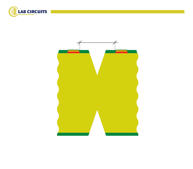
|
Min. 1,0 mm. | Min. 0,75 mm. |
| Scoring positioning | 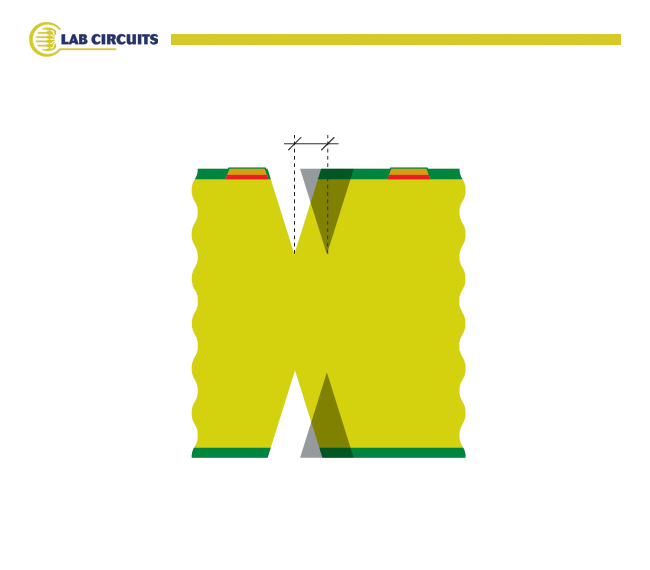
|
±0,10 mm | ±0,075 mm |
| Scoring remaining thickness | 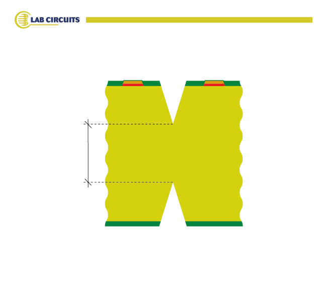
|
±0,15 mm
|
±0,075 mm
|
| Board size | 
|
± 0,15 mm.
|
± 0,10 mm. |
| Total thickness tolerance | 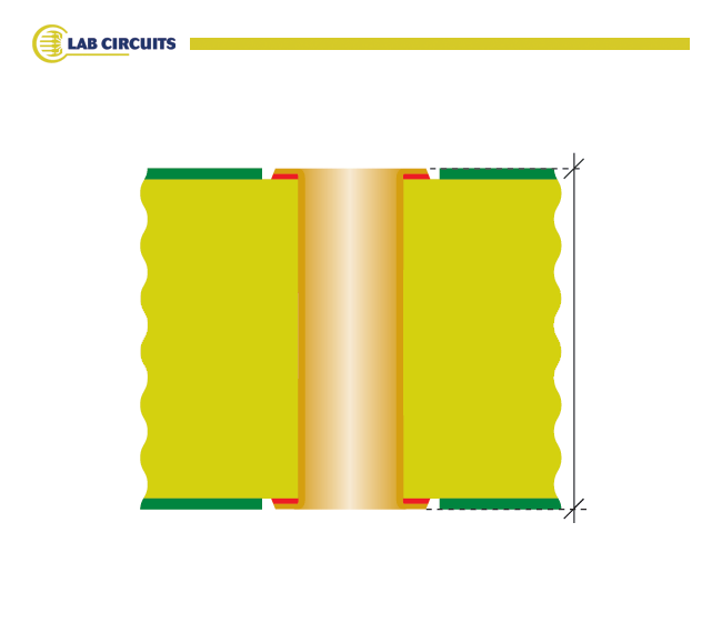
|
±10 % | ±5 % |
| Finished plated hole copper thickness | 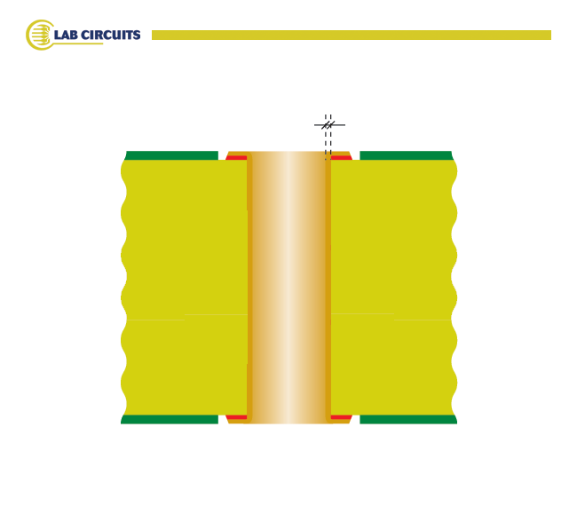
|
Average: 25 µm
Minim: 20 µm |
Average: 35 µm
Mínim: 30 µm |
| Mínimum wall between same net plated through holes | 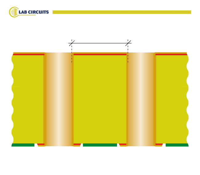
|
0.30 mm | 0.25 mm |
| Minimum wall between different net plated through holes | 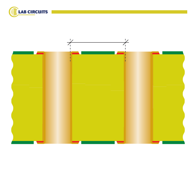
|
0,40 mm. | 0,35 mm. |
| Minimum wall between non plated through holes | 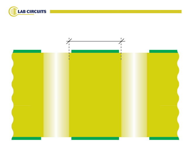
|
0,25 mm. | 0,20 mm. |
| Minimum annular ring non plated hole | 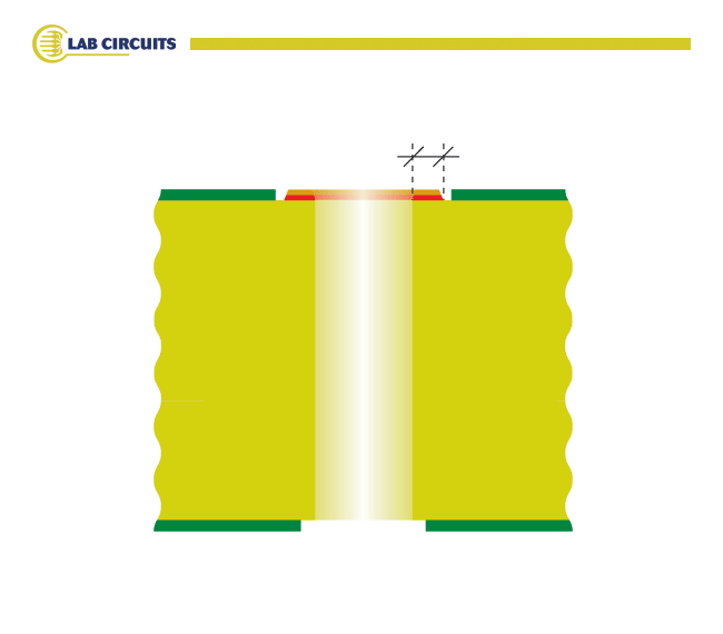
|
0,25 mm
|
0,20 mm
|
| Track to non plated through hole minimum spacing | 
|
0,20 mm
|
0,15 mm
|
| Track to board edge minimum spacing | 
|
0,20 mm
|
0,15 mm
|
| Offset between board edge and drill | 
|
Max. 0,15 mm.
|
Max. 0,10 mm.
|
| Drill to pad misalingnement | 
|
Max. 0,10 mm.
|
Max. 0,075 mm.
|
| Soldermask feature tolerance | 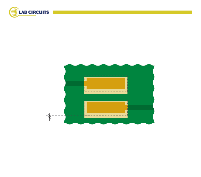
|
Max. 0,15 mm. | Max. 0,075 mm. |
| Soldermask min Dam size on fiber | 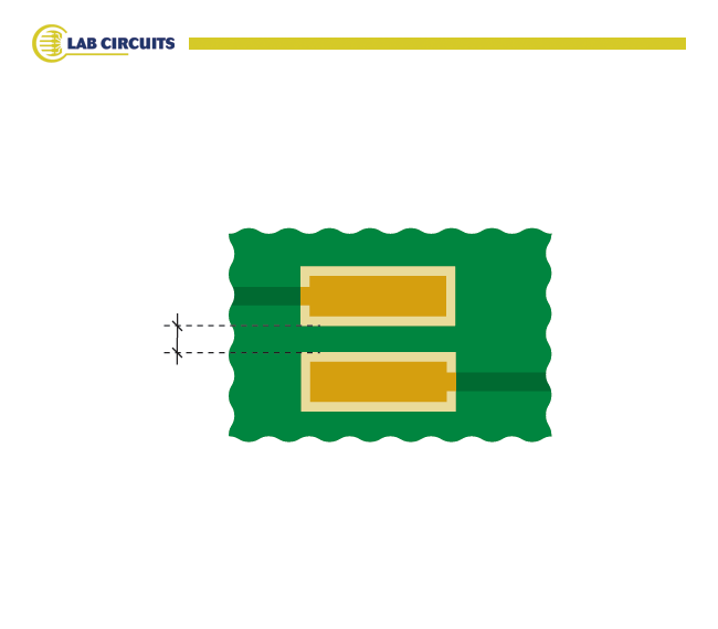
|
SOLDERMASK GREEN COLOR
Damm 70µm if final copper thickness is 17÷54µm. Damm 85µm if final copper thickness is 55÷85µm. Damm 105µm if final copper thickness is 86÷155µm. SOLDERMASK WHITE COLOR Damm 110µm if final copper thickness is 17÷54µm. Damm 110µm if final copper thickness is 55÷85µm. Other final copper thickness > 85µm, to consult. OTHER SOLDERMASK COLORS Damm 80µm if final copper thickness is 17÷54µm. Damm 95µm if final copper thickness is 55÷85µm. Damm 105µm if final copper thickness is 86÷155µm. |
-- |
| Photoimageable soldermask clearance | 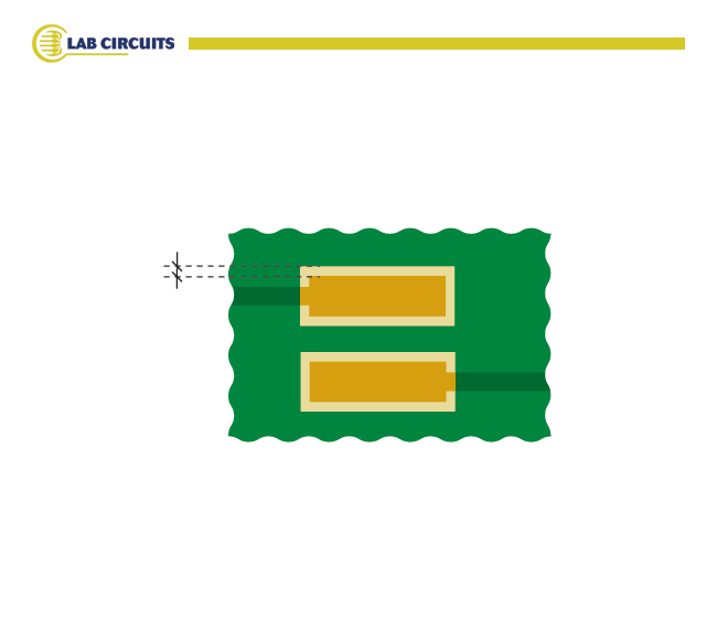
|
0,07 mm
|
0.06 mm |
| Silkscreened soldermask clearance |
|
0,20 mm
|
0,15 mm
|
| Legend minimum line | 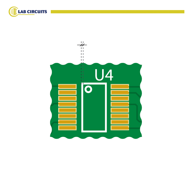
|
0,125 mm
|
0,10 mm
|
| Conductive ink (graphite) overlapping | 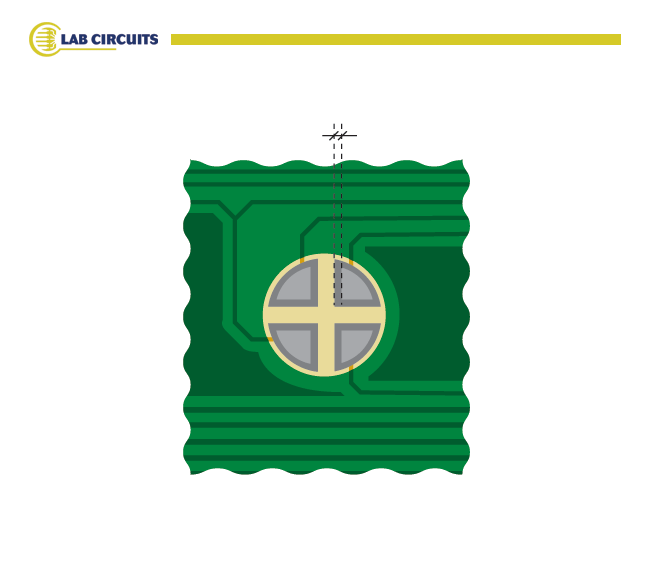
|
0,20 mm
|
0,125 mm
|
| Conductive ink (graphite) spacing | 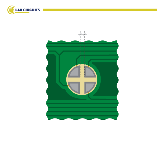
|
0,50 mm | 0,40 mm |
| Conductive ink to pad spacing | 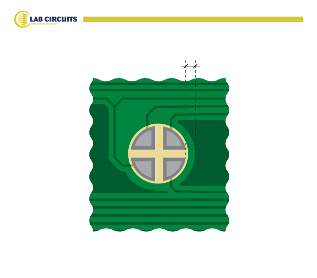
|
0,40 mm | 0,30 mm |
| Peel-off mask overlapping | 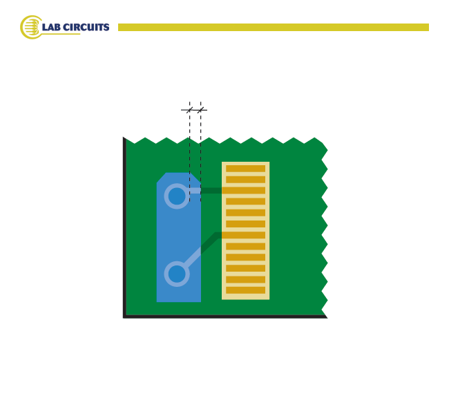
|
0.8 mm
|
0,50 mm
|
| Peel-off mask to pad spacing | 
|
1 mm | 0,70 mm |
| Peel-off mask to board
edge spacing |
|
1 mm | 0,70 mm |
| Maximum peel-off mask filled hole | 
|
1.8 mm | 2 mm |
| Bow and twist | Maxim 1% | Maxim 0,5 % | |
| Insulation resistance | Minim 0,5 MOhm | Minim 2,0 MOhm | |
| Continuity | Maxim 10 Ohms | - | |
| Ionic contamination | Max. 0,4 µg Eq. NaCl/cm² | Max. 0,4 µg Eq. NaCl/cm² | |
| For other features | See spec.
IPC-A-600 Rev K jul-20 |
- |
Last update: 12-06-2023
Units: Milimeters
| STANDARD | SPECIAL | ||
|---|---|---|---|
| Trace / spacing width |
|
±20% (½ oz )
±25% (1-2 oz ) |
±10% (½ oz )
±15% (1 - 2 oz) |
| Plated hole diameter |
|
+4 mil / -2 mil
(or equivalent) |
+4 mil / -0,0 mil
±2 mil |
| Non plated hole diameter |
|
+4 mil / -0,0 mil
(or equivalent) |
±1.4 mil
(or equivalent) |
| Castellated plated holes |
|
Total thickness circuit.....................>= 0,02 mil
Cross annular ring.......... detall - A >= 0,02 mil Minimum diameter..........detall - B >= 0,02 mil Longitudinal annular...... detall - C >= 0,006 mil Annular separation.........detall - D >= 0,006 mil Edge separation..............detall - E >= 0,08 mil |
- |
| Scoring to copper clearance |
|
Min. 40 mil. | Min. 30 mil |
| Scoring positioning |
|
± 4 mil | ± 3 mil |
| Scoring remaining thickness |
|
± 4 mil
|
± 2 mil
|
| Board size |
|
± 6 mil.
|
± 4 mil. |
| Total thickness tolerance |
|
±10 % | ±5 % |
| Finished plated hole copper thickness |
|
Average: 0.7 oz
Minimum: 0.6 oz |
Average: 1 oz
Minimum: 0.86 oz |
| Minimum wall between same net plated through holes |
|
12 mil. | 10 mil. |
| Minimum wall between different net plated through holes |
|
16 mil. | 14 mil. |
| Minimum wall between non plated through holes |
|
10 mil. | 8 mil. |
| Minimum annular ring non plated hole |
|
10 mil.
|
8 mil. |
| Track to non plated through hole minimum spacing |
|
8 mil. | 6 mil. |
| Conductor to board edge
minimum spacing |
|
8 mil. | 6 mil. |
| Offset between board edge and drill |
|
Max. 6 mil.
|
Max. 4 mil.
|
| Offset between drill to outlayer pad |
|
Max. 4 mil.
|
Max. 3 mil.
|
| Soldermask feature tolerance |
|
Max. 6 mil. | Max. 3 mil. |
| Soldermask minimum Dam size on fiber |
|
SOLDERMASK GREEN COLOR
Damm 2,75mil if final copper thickness is 0.66÷2.12mil. Damm 3,35mil if final copper thickness is 2.16÷3.35mil. Damm 4,13mil if final copper thickness is 3.38÷6.10mil. SOLDERMASK COLOR BLANCO Damm 4,33mil if final copper thickness is 0.66÷2.12mil. Damm 4,33mil if final copper thickness is 2.16÷3.35mil. Other final copper thickness > 3.35mil, to consult. OTROS COLORES SOLDERMASK Damm 3,15mil if final copper thickness is 0.66÷2.12mil. Damm 3,75mil if final copper thickness is 2.16÷3.35mil. Damm 4,13mil if final copper thickness is 3.38÷6.10mil. |
- |
| Photoimageable soldermask clearance |
|
3 mil. | 2.36 mil. |
| Silkscreened soldermask clearance |
|
8 mil. | 6 mil. |
| Legend minimum line |
|
5 mil. | 4 mil. |
| Conductive ink (graphite) overlapping |
|
8 mil.
|
5 mil. |
| Conductive ink (graphite) spacing |
|
20 mil. | 16 mil. |
| Conductive ink to pad spacing |
|
16 mil. | 12 mil. |
| Peel-off mask overlapping |
|
32 mil. | 20 mil. |
| Peel-off mask to pad spacing |
|
40 mil. | 28 mil. |
| Peel-off mask to board
edge spacing |
|
40 mil. | 28 mil. |
| Maximum peel-off mask filled hole |
|
71 mil. | 79 mil. |
| Bow and twist | Maxim 1% | Maxim 0,5 % | |
| Insulation resistance | Minimum 0,5 MOhm | Minimum 2,0 MOhm | |
| Continuity | Maxim 10 Ohms | - | |
| Ionic contamination | Max. 1µg Eq. CINa/cm2 | Max. 0,8 µg Eq. CINa/cm2 | |
| Other features | See spec.
IPC-A-600 Rev K jul-20 |
- |
Last update: 12-06-2023
Units: Mils
© Lab circuits 2026 · Legal note · Cookies · Site map · Credits